Features
Fully automated
Multi-tech XPS / HAXPES
- Easy Operation & Multi-technique Options
- High Performance Large & Micro Area XPS Analysis
- High Speed & Non Destructive Depth Profiling
- Fully Automated with Sample Parking
- Hard X-ray Cr Kα source for HAXPES
- Comprehensive solution for batteries, semiconductors, organic devices and other applications
Ease of Operation

PHI GENESIS provides a new user interface experience that enables intuitive, easy and fully automated operation of the high-performance instrument with a new UI.
This interface allows access to all necessary functions to setup routine and advanced multi-technique acquisitions within a single screen, while retaining functions such as navigation using intro photo and 100% accurate positioning from X-ray induced secondary electron images (SXI).

Intuitive UI
PHI GENESIS provides a simple, intuitive and ease of use user interface. This allows users to perform simple operations as well as automated analyses including all options.
Multi-Technique Options

Same area automated analysis using multiple techniques covering full range of energy - from conduction band with LEIPS to core-level excitation with HAXPES, PHI GENESIS offers unprecedented value not found in conventional XPS instruments.
No compromise solution:
The high-performance XPS, HAXPES, UPS, LEIPS, REELS, AES, and a variety of other options meet all surface analysis needs.
High Throughput Large Area Analysis

The newly designed high-sensitivity analyzer enables high throughput analysis for both XPS and HAXPES.
Superior Micro Area Spectroscopy
In PHI GENESIS, micro-focused scanning X-ray source is used for intuitive SEM-like navigation using X-ray induced secondary electron images (SXIs). Multi-point small areas can be defined from SXI images with 100% certainty for spectra, depth profiles and maps.
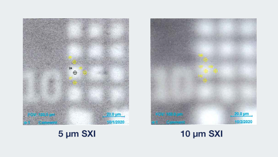
Improved Scanning X-ray Image(SXI)
The unsuppressed 5 µm small spot X-ray beam opens new opportunities for micro-XPS applications.
High Throughput Depth Profiling
PHI GENESIS enables high throughput depth profiling. Micro-focused X-ray source, highly sensitive detector, high-performance Argon ion gun, and high-efficiency dual beam neutralization enable fully automated depth profiling, including multi-point analysis within a single crater.
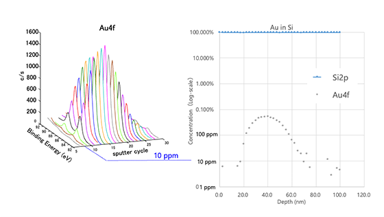
High sensitivity during depth profiling
Sample: Au ion-implanted Si wafer with as small as 10 ppm Au detected in during depth profiling
Non Destructive Depth Profiling
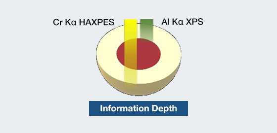
Using high-energy hard X-ray source, it is possible to obtain information from a deeper depth compared to conventional soft X-ray XPS.
This enables a detailed and unperturbed chemical state analysis of buried interfaces without sputtering.
No-sputter depth probing
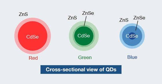
Quantum Dots(QDs) with a diameter of approximately 10 to 50 nm are used in a next-generation transparent luminescent materials.
By combining information from same area analysis using XPS (Al Kα X-rays) and HAXPES (Cr Kα X-rays), it is possible to perform detailed depth-resolved structure analysis of QDs.
Combination of XPS and HAXPES allows depth-resolved, quantitative and chemical analysis of nanoparticles, eliminating possible ion beam-induced damage.
List of Application Area
Advanced functional materials used in all-solid-state batteries, semiconductors, photovoltaics, catalysts, etc. are complex multi-component materials, and their research and development relies on high throughput quantitative chemical structure-to-property optimization.
ULVAC-PHI offers new surface analysis instrument that offers unsuppressed high performance and high degree of flexibility and automation to meet the requirements of all customers - the "PHI GENESIS" scanning X-ray photoelectron spectrometer (XPS).
The Application Areas include:
- semiconductors, batteries, organic devices, catalysts, quantum dots, nanoparticles, bio- and life science materials, polymers, ceramics, metals, and others solid materials and devices.
Wide Variety of XPS Options of Research Needs
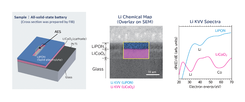
Battery
“pA-AES Lithium chemical map from LiPON/LiCoO2 cross-section”
Li-based materials, such as LiPON, are sensitive to electron beam irradiation.
High-sensitivity analyzer available at PHI GENESIS enables fast acquisition of AES chemical maps at low beam current (300 pA).
Semiconductors
Semiconductor devices generally consist of complex thin films containing many elements, and their development often requires non-destructive analysis of chemical states at interfaces.
HAXPES is necessary to acquire information from buried interfaces such as GaN under gate oxide film.

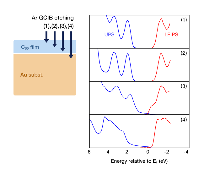
Organic Devices
The change of energy band diagram using UPS/LEIPS and Ar-GCIB
(1) C60 film surface
(2) C60 film after surface cleaning.
(3) C60 film /Au interface
(4) Au surface
Energy diagram of organic layers as a function of depth can be determined by combination of UPS/LEIPS and Ar-GCIB depth profiling.
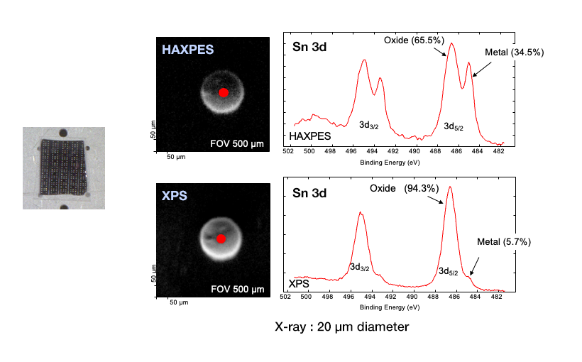
Micro Electronics
Micro-spot solder-ball analysis
The HAXPES data shows a higher percentage of metallic Sn than the XPS data. This is consistent with the formation of surface oxides on the solder ball.